FPGA

FPGA, (Field-programmable gate array)
a field-programmable integrated circuit consisting of a two-dimensional array of logic blocks interconnected by a hierarchy of reconfigurable routing channels. The behavior of a FPGA is defined by a schematic design or by a hardware description language (HDL), most notably VHDL and Verilog. FPGA cards of their main suppliers Xilinx [2] and Altera [3] can be plugged into a PC with communication over the PCI or PCI Express bus. IBM's POWER8 processor, introduced in August 2013, features a CAPI port (Coherent Accelerator Processor Interface) is layered on top of PCI Express 3.0 suited to connect custom hardware such as FPGAs [4] [5].
Contents
Architecture
Structure
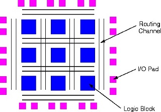 |
The structure is a two-dimensional array of logic blocks and reconfigurable routing channels, which all have the same width (number of wires). I/O pads can connect to any one of the wiring segments in the channel adjacent to it [6]. |
| FPGA structure [7] |
Blocks and Cells
 |
Each logic block (configurable logic block CLB, or logic array block LAB) consists of one or more logical cells (LC, adaptive logic module ALM, logic element LE, Slice etc.), each with a n-input bits (4-6) to one-output bit programmable lookup table (LUT) - the combinatorial logic, and a D-Flip-Flop, which synchronizes and stores the output by the edge of a clock signal to implement a sequential logic. A configurable multiplexer either switches the direct or latched LUT output outwards. |
| Logic cell with LUT and D-Flip-Flop [8] |
Routing
 |
Inputs and outputs of a cell can connect to any one of the routing wires in the channel adjacent to it. Whenever a vertical and a horizontal channel intersect there is a switch box with programmable switches that allow it to connect to other wires in adjacent channel segments. Xilinx Virtex devices further provide BlockRAM, a 4096-bit synchronous memory which can be configured for single or dual port usage with variable widths of 1, 2, 4, 8 or 16 bits. |
| Switch box topology [9] |
FPGA in Computer Chess
FPGAs are suited to implement a Belle like move generator in hardware. While Marc Boulé proposed a pure generation approach as used by his program MBChess, Chrilly Donninger, with PCI-communication overhead in mind, went some steps further in Brutus [10] and Hydra, using a complete 3-ply iterative search including quiescence and evaluation, controlled by a finite state machine (FSM).
Boulé
In his Masters thesis [11], Marc Boulé proposed a FPGA move generator, as used by his chess program MBChess. His approach performs a Belle like move masking method with find victim and find aggressor cycles in MVV-LVA manner. A 1-bit, 64-deep synchronous memory in each square is used to memorize masked bits. The move generator includes a PCI interface to connect it to the PC running MBChess. Communication is done via different commands, such as to instruct the move generator to undo the currently stored move, generate and return the next move and execute that move on its internal FPGA board representation. In total, 10,804 out of 18,816 logic cells of a Xilinx XCV800 [12] were used, 10,104 as LUT, 700 as RAM [13].

A block diagram of a chess square with transmitter (TX) and the receiver (RX) [14]
Donninger
Brutus [15] and its successor Hydra by Chrilly Donninger et al. [16] perform the last 3 plies of an n-ply search on the FPGA side, inclusively the quiescence search and evaluations. It uses 67 out of 96 BlockRAMs, 534 of 24,576 Flip-Flops, and 18,403 of 24,576 LUTs. An upper bound for the number of cycles per search node is 9. Hydra essentially contains a big piece of combinatorial logic, controlled by a finite state machine (FSM) with 54 states for the search. The move generator consists of the generate aggressor module and the generate victim module, both instantiate 64 square modules, one for each square.
The squares send piece-signals if any, respectively forwarding the signals of sliding pieces. Each square can output the signal ’victim found’ to indicate the ’victim’ is target square of a pseudo-legal move. The collection of all ’victim found’ signals is the input for a comparator tree, an arbiter, which selects the most attractive, not yet examined victim. The Generate Aggressor module takes the arbiter’s output as input and sends the signal of a super-piece from the target to find one or more origin squares. Selection criteria are the values of attacked pieces and whether or not a move is a killer move.
Publications
1997 ...
- Kurt Keutzer (1997). Challenges in CAD for the One Million Gate FPGA. FPGA 1997, pdf
- Stephen Brown, Zvonko Vranesic (1999). Fundamentals of Digital Logic with VHDL Design. McGraw-Hill
2000 ...
- Youhei Hori, Minenobu Seki, Tsutomu Maruyama, Reijer Grimbergen, Tsutomu Hoshino (2000). A Shogi Processor with a Field Programmable Gate Array. CG 2000
- Valavan Manohararajah, Terry P. Borer, Stephen Brown, Zvonko Vranesic (2002). Automatic Partitioning for Improved Placement and Routing in Complex Programmable Logic Devices. FPL 2002
- Marc Boulé (2002). An FPGA Move Generator for the Game of Chess. Masters thesis, McGill University, supervisor: Zeljko Zilic, co-supervisor: Monty Newborn
- Marc Boulé, Zeljko Zilic (2002). An FPGA Move Generator for the Game of Chess. McGill University
- Marc Boulé, Zeljko Zilic (2002). An FPGA Move Generator for the Game of Chess. ICGA Journal, Vol. 25, No. 2
- Youhei Hori, Masashi Sonoyama, Tsutomu Maruyama (2002). An FPGA-Based Processor for Shogi Mating Problems. 2002 IEEE International Conference on Field-Programmable Technology, 2002, pdf
- Marc Boulé, Zeljko Zilic (2003). FPGA Hardware Acceleration: From Chess Playing to Automated Theorem Proving. poster presentation, Micronet Sept. 2003
- Stephen Brown, Zvonko Vranesic (2003). Fundamentals of Digital Logic with Verilog Design. McGraw-Hill
- Chrilly Donninger, Alex Kure, Ulf Lorenz (2004). Parallel Brutus: The First Distributed, FPGA Accelerated Chess Program. IPDPS’04
- Chrilly Donninger, Ulf Lorenz (2004). The Chess Monster Hydra in Field Programmable Logic and Application, FPL 2004
2005 ...
- Valavan Manohararajah (2005). Area Optimizations in FPGA Architecture and CAD. Ph.D. Thesis, pdf
- Valavan Manohararajah, Stephen Brown, Zvonko Vranesic (2006). Adaptive FPGAs: High-Level Architecture and a Synthesis Method. FPL 2006, pdf
- Valavan Manohararajah, Stephen Brown, Zvonko Vranesic (2006). Heuristics for Area Minimization in LUT-Based FPGA Technology Mapping. IEEE Transactions on CAD of Integrated Circuits and Systems, Vol. 25, No. 11
- Stephen Brown, Zvonko Vranesic (2007). Fundamentals of Digital Logic with Verilog Design. McGraw-Hill, 2nd edition, amazon
- Stephen Brown, Zvonko Vranesic (2008). Fundamentals of Digital Logic with VHDL Design. McGraw-Hill, 3rd edition, amazon
- Zeljko Zilic (2009). Designing and Using FPGAs beyond Classical Binary Logic: Opportunities in Nano-Scale Integration Age. ISMVL 2009
2010 ...
- James Bowman (2010). J1: a small Forth CPU Core for FPGAs. EuroForth 2010, pdf [17]
- Edin Kadric, Naraig Manjikian, Zeljko Zilic (2012). An FPGA implementation for a high-speed optical link with a PCIe interface. SoCC 2012
- Franjo Plavec, Zvonko Vranesic, Stephen Brown (2013). Exploiting Task- and Data-Level Parallelism in Streaming Applications Implemented in FPGAs. TRETS, Vol. 6, No. 4
2015 ...
- António Coelho (2016). FPGA Multiprocessor for Game Tree Searches. M.Sc. thesis, Instituto Superior Técnico, University of Lisbon, pdf » Faile
2020 ...
- Terry Loesch (2020). Designing an FPGA Chess Engine. amazon
Forum Posts
2000 ...
- Chip design project & another request for Belle/DT/DB info by Tom Kerrigan, CCC, January 27, 2000 » Belle, Deep Thought, Deep Blue
- FPGA move generator by Ties Bos, rgcc, September 06, 2000
- A Response From Marc Boule by Slater Wold, CCC, April 02, 2002
- Re: Thesis by Marc Boule by Marc Boulé, CCC, September 08, 2002
- Re: Attention - Slater Wold by Marc Boulé, CCC, April 10, 2003
- Go Brutus!! by Pete Rihaczek, CCC, November 24, 2003
2005 ...
- fpga/mcu implementation by Daniel Staf, CCC, May 31, 2005
- FPGA cards and RYBKA by albitex, Rybka Forum, July 11, 2007
2010 ...
- FPGA chess by Matthew Lai, CCC, November 26, 2014
External Links
- Programmable Logic/FPGAs from Wikibooks
- Hamsterworks Wiki!
- The FPGA Place-and-Route Challenge by Vaughn Betz
- The J1 Forth CPU — excamera » Forth
- UCLA Computer Science Department | Winter 2004 | CS 151C - Design of Digital Systems | VHDL Projects on XSV Board
- FPGA Snake game uses no VHDL at all - Hack a Day
- The General FPGA-based board game machine, a prototype by Antti Karttunen
- What is Brutus?, ChessBase News, March 20, 2002
- All about the Hydra chess project, ChessBase News, August 22, 2004
Vendors
- FPGA CPLD and ASIC from Altera
- All Programmable Technologies from Xilinx Inc.
- Alpha Data - High Performance Computing with Xilinx Virtex-7 FPGAs
Misc
- Toto Blanke - PPG, Electric Circus (1977) feat. Edward Vesala, Jasper van 't Hof, YouTube Video
References
- ↑ FPGA from Wikipedia
- ↑ All Programmable Technologies from Xilinx Inc.
- ↑ FPGA CPLD and ASIC from Altera
- ↑ IBM Power8 Processor Detailed - Features 22nm Design With 12 Cores, 96 MB eDRAM L3 Cache and 4 GHz Clock Speed
- ↑ Re: FPGA chess by Milos Stanisavljevic, CCC, November 28, 2014
- ↑ FPGA Architecture for the Challenge
- ↑ FPGA Architecture for the Challenge
- ↑ Field Programmable Gate Array from Wikipedia.de (German)
- ↑ Field-programmable gate array from Wikipedia
- ↑ What is Brutus?, ChessBase News, March 20, 2002
- ↑ Marc Boulé (2002). An FPGA Move Generator for the Game of Chess. Masters thesis, McGill University, supervisor: Zeljko Zilic, co-supervisor: Monty Newborn
- ↑ Re: Attention - Slater Wold by Marc Boulé, CCC, April 10, 2003
- ↑ Re: Thesis by Marc Boule by Marc Boulé, CCC, September 08, 2002
- ↑ Marc Boulé (2002). An FPGA Move Generator for the Game of Chess. Masters thesis, McGill University, supervisor: Zeljko Zilic, co-supervisor: Monty Newborn
- ↑ Chrilly Donninger, Alex Kure, Ulf Lorenz (2004). Parallel Brutus: The First Distributed, FPGA Accelerated Chess Program. IPDPS’04, pdf
- ↑ Chrilly Donninger, Ulf Lorenz (2004). The Chess Monster Hydra in Field Programmable Logic and Application, 14th International Conference, FPL 2004
- ↑ The J1 Forth CPU — excamera